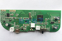
The microstructure of the solder joint is affected by the process used. Under all other conditions being equal ----- The same alloy with the same PCB welding surface treatment, the same components, the microstructure of the solder joint will change with the change of process parameters. For a known system, the process parameters that affect the microstructure formation of solder joints in the SMT patch processing process include heating parameters and cooling parameters.
1, heating parameters
In the heating phase of the welding process, the parameters that play a key role are the peak temperature and the time that the temperature is above the liquidus. Higher peak temperature or longer liquidus time will cause excessive intermetallic compounds to form at the interface and inside the solder joint. Under conditions that promote the formation of excessive intermetallic compounds, the thickness of intermetallic compounds at the interface increases. When the peak temperature is high enough and the temperature is higher than the liquidus for longer, the intermetallic compounds will increase and migrate to the inside of the pcb solder joint.
In extreme cases, intermetallic compounds can appear on the free surface of the solder, causing a change in the appearance of the solder joint. The change of appearance directly reflects the change of microstructure. It can be expected that the mechanism and phenomenon of all three forms of intermetallic compounds will have an adverse effect on the solder joint, either in terms of the appearance of the solder joint, or in terms of the mechanical properties of the solder joint. It must be pointed out that the coating properties of the PCB pad and the gold affinity of the solder composition may affect the formation of the solder joint microstructure. Such as tin leaching, silver leaching, OSP, HASL surface treatment, they participate in the interface reaction is Cu, its diffusion rate in molten Sn is 8.6 times that of Ni, easy to form a relatively thick IMC layer, and ENIG surface treatment formed NiSn intermetallic compound thickness is relatively thin.
2. Cooling parameters
The faster the cooling rate, the smaller the microstructure formed. For tin-lead eutectic alloys, the slow cooling rate brings the microstructure closer to the equilibrium state.
The microstructure of eutectic solder is usually composed of a characteristic thin layer aggregate of 63Sn/37Pb. With the increase of cooling rate, the degradation of thin layer aggregate structure increases and eventually disappears. For PCBA lead-free solder, such as SAC, the faster cooling rate also results in finer tin grains. It is generally accepted that an increase in the cooling rate results in a finer grain (metallographic) structure in the tin block, but this general rule is often complicated by the metalworking reaction at the interface boundary and solder joint interface.